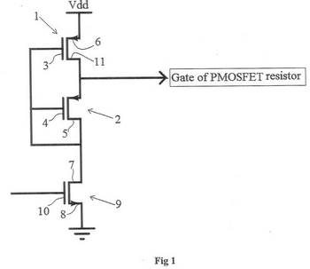
 A biasing circuit for a PMOSFET resistor for compensating process, voltage and
temperature (PYT) variations affecting the resistance of the PMOSFET resistor
comprising a pair of series connected first (1) and second (2) PMOSFETs. Gates (3 &
4) of both (1 & 2) the PMOSFETS are connected to a drain (5) of the second
PMOSFET (2). Source (6) of the first PMOSFET (1) is tied to a voltage supply
source, drain (7) of a third PMOSFET (9) is connected to the drain (5) of the second
PMOSFET (2) and source (8) of the third PMOSFET (9) is grounded. The third
PMOSFET (9) is biased appropriately at a gate (10) thereof. The output of the biasing
circuit is taken at the drain (11) of the first PMOSFET (1) and fed to a gate of the
PMOSFET resistor. (Fig 1) A biasing circuit for a PMOSFET resistor for compensating process, voltage and
temperature (PYT) variations affecting the resistance of the PMOSFET resistor
comprising a pair of series connected first (1) and second (2) PMOSFETs. Gates (3 &
4) of both (1 & 2) the PMOSFETS are connected to a drain (5) of the second
PMOSFET (2). Source (6) of the first PMOSFET (1) is tied to a voltage supply
source, drain (7) of a third PMOSFET (9) is connected to the drain (5) of the second
PMOSFET (2) and source (8) of the third PMOSFET (9) is grounded. The third
PMOSFET (9) is biased appropriately at a gate (10) thereof. The output of the biasing
circuit is taken at the drain (11) of the first PMOSFET (1) and fed to a gate of the
PMOSFET resistor. (Fig 1)
Indian patent application no. 1198/MUM/2012
Inventors: Maryam Shojaei Baghini, Anvesha A
|
